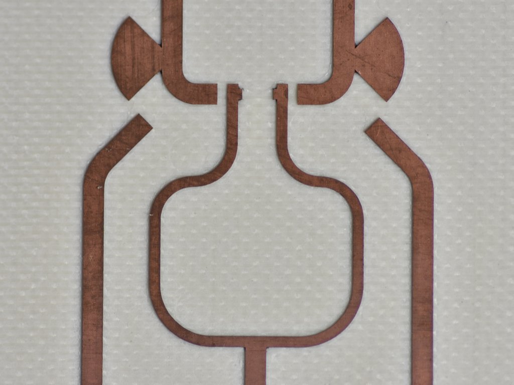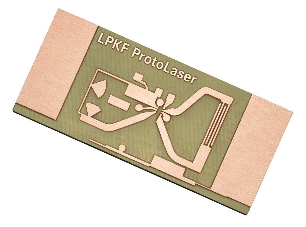
Milling the conductor pattern
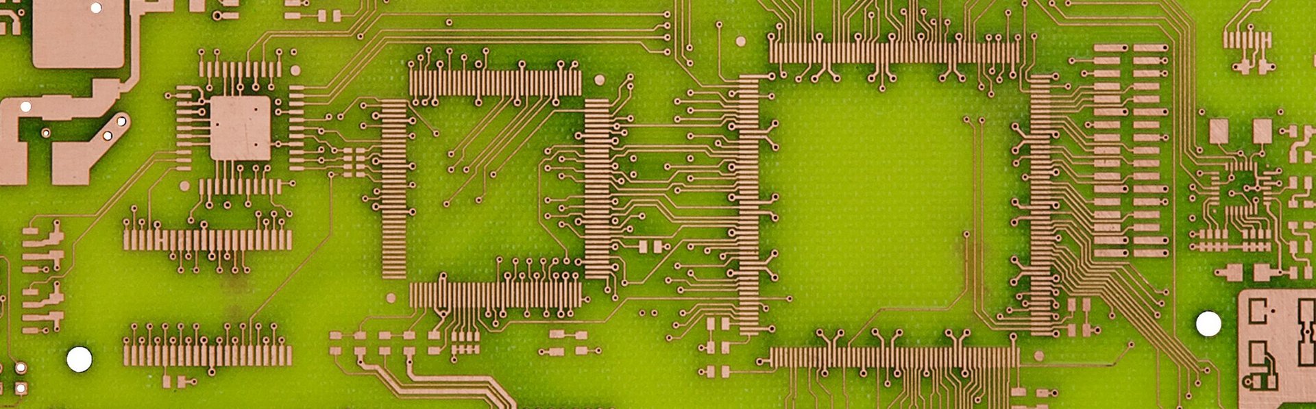
1- & 2-sided PCBs and multilayers
Mechanical and laser systems selectively remove the copper layers on single- and double-sided circuit boards, thereby creating insulating channels that precisely delineate the required conductive traces and pads. The circuit board plotters also drill all the necessary holes in the boards.