
Solutions for the semiconductor industry
Empowered by several decades of laser processing experience, LPKF offers leading-edge solutions with system benefits such as higher precision and yield as well as cost efficiency, supporting the ever ongoing trend towards miniaturization. The portfolio incorporates numerous features:
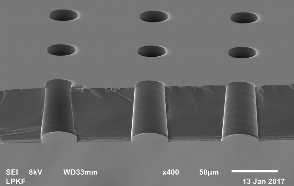
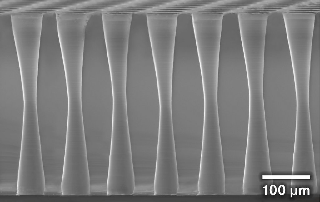
A new method to produce through glass vias (TGVs) helps to unlock the full potential of thin glass substrates Conductor tracks on epoxy mold Compounds (EMCs) and through mold vias (TMVs) enable new package design approaches Laser cutting and drilling of a wide range of materials are possible. The laser tool has become a necessity for applications on the micron scale.
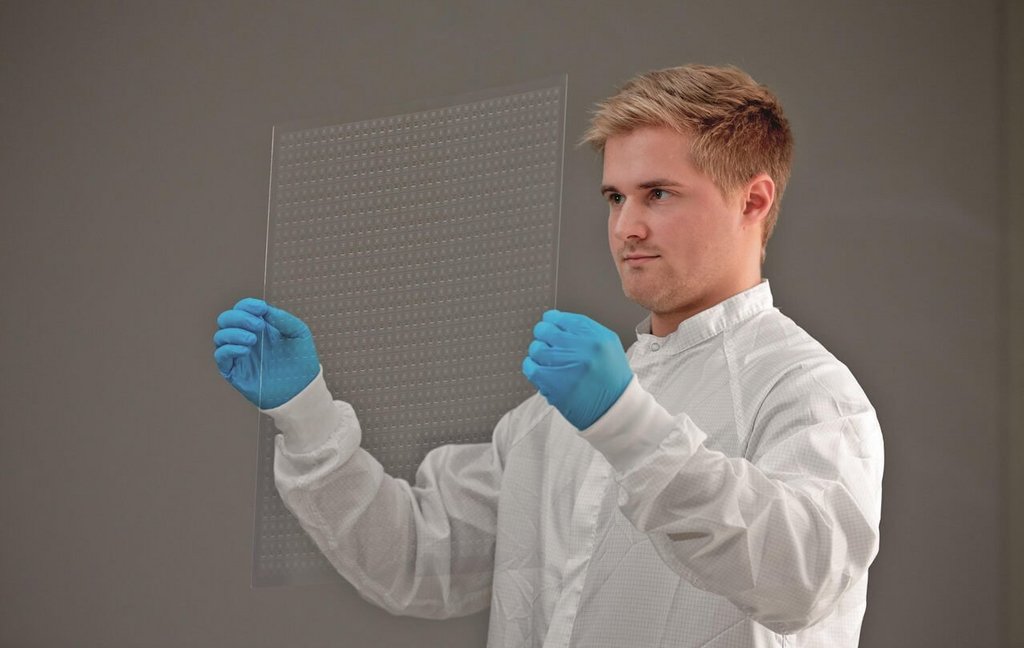
Through glass vias (TGV)
Thin glass with a thickness of 50 µm to 500 µm is very suitable as a substrate material for high-density, high-frequency applications.
The new LIDE process from LPKF uses the laser as a noncontact precision tool for micromachining through glass vias with unrivaled productivity and quality.
Vitrion -- Your specialized glass foundry
Various concepts are available for the implementation of TGV in your projects -- bundled under the Vitrion brand.
Vitrion enables prototyping and a series production service for a wide range of thin glass applications in a previously unreached quality. Use it to your advantage.
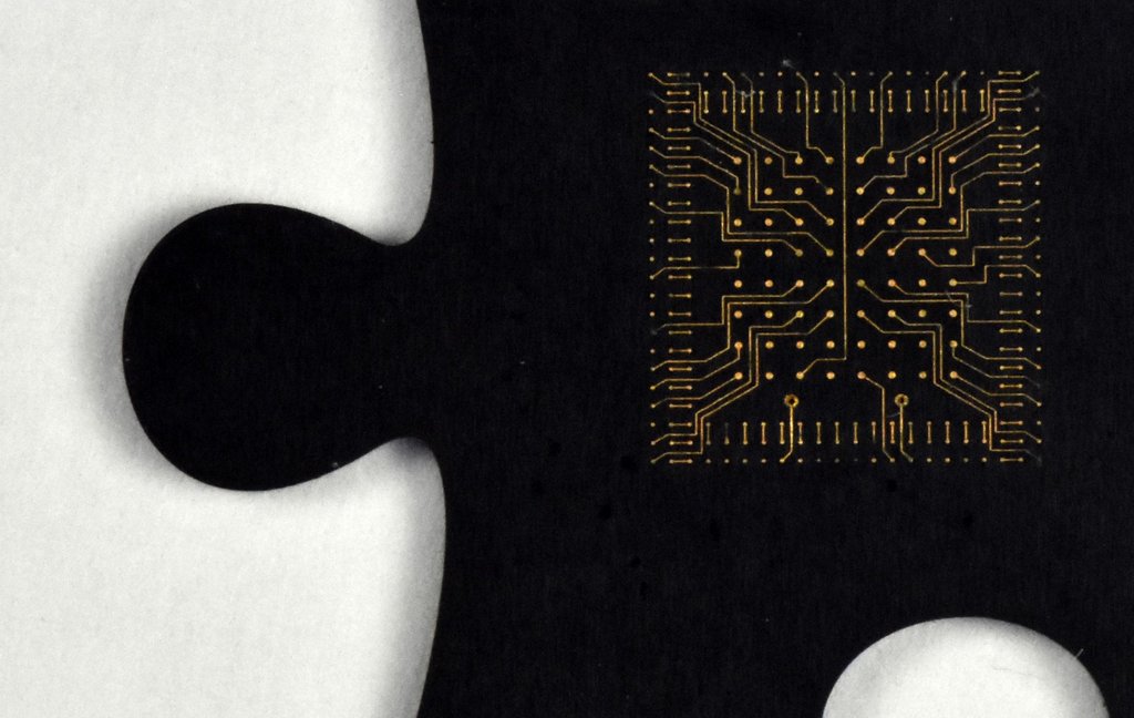
Processing of Mold Compounds with Active Mold Packaging (AMP) Technology
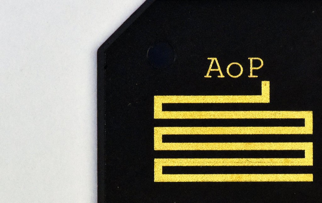
In many cases, the performance of the IC is limited by the IC package. As a result, a great deal of attention is being devoted to improving IC packaging technology to meet these challenges. The Laser Direct Structuring (LDS) technology in epoxy mold compounds (EMCs) enables an increased IC package functionality. The applications include Antenna-on-Package (AoP) designs for 5 GHz and beyond, Package-on-Package (PoP) designs for reduced package heights, and full or compartment EMI shielding for increased package performance.
The outer package surface can be utilized, walls can be used as a circuit carrier, and through-hole plating can be created in a cost-efficient and safe manner. The LDS method uses lasers to apply conductor structures onto plastic bodies, which are later chemically metallized.
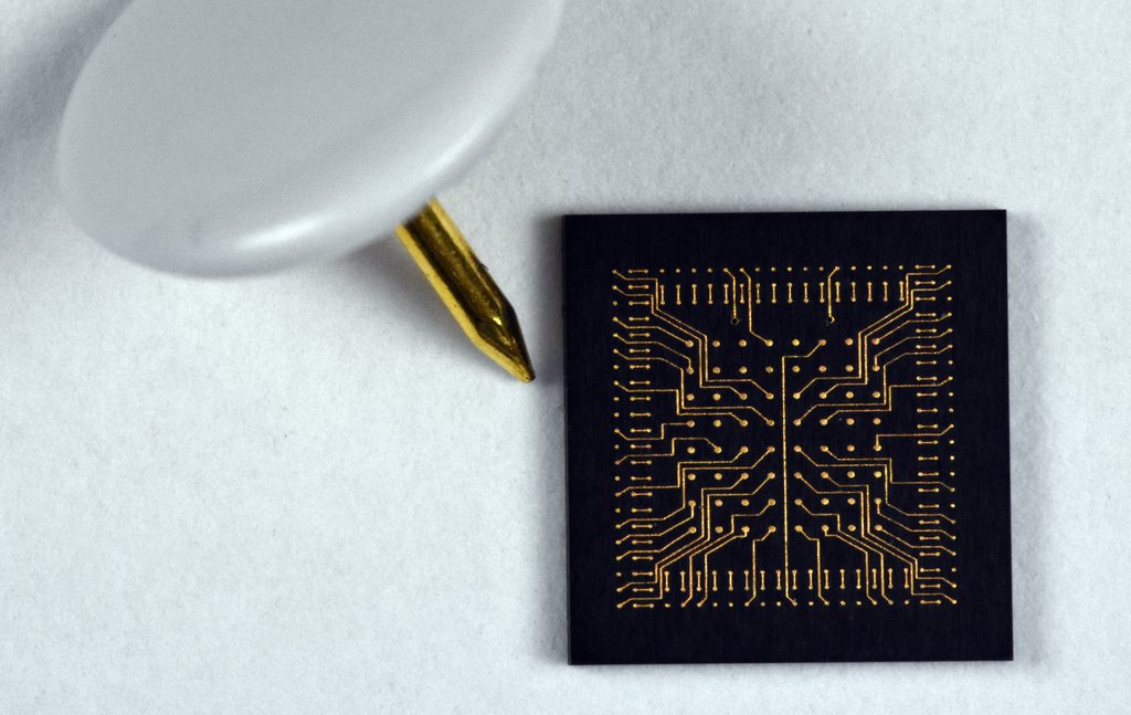

LDS has the potential to replace the traditional process of contact creation because it creates the contacts directly during the mold and laser process. The contacts and the tracks are activated and coated together in a single step.
Changes to the circuit layout can be easily implemented through changing of the laser path. LPKF LDS technology thus opens up additional platform strategies for sensor and chip packages.
Through mold vias (TMV)
The constant drive towards further miniaturization and heterogeneous system integration is leading to a need for new packaging technologies that allow 3D integration with the potential for low-cost applications.
The use of the LDS (Laser Direct Structuring) interconnect technique for through mold vias (TMVs) in multichip embedding is derived from high-volume mechatronic integrated device (MID) manufacturing with a focus on high functionality integration. The LDS technology makes it possible to drill vias and prepare them for electrolytic metallization at the same time.
Singulation of IC Packages
Materials used in the construction of IC packages are of great importance. Their physical, electrical, and chemical properties establish the foundation of the package, and ultimately its performance limits. LPKF's application and development teams have gained a deep understanding of laser drilling and cutting of both organic and inorganic substrates used in the electronics industry. The laser systems specifically tailored to the needs of the electronics industry are capable of cutting and opening or drilling a variety of IC compounds:
- Curved cuts with extremely fine outlines
- Clean side walls
- Virtually no burring
- Small heat-affected zone (HAZ)
- High positioning precision
Our engineers would be happy to support you in your evaluation phase as well during ramp-up and high-volume production. Learn more about what is possible.