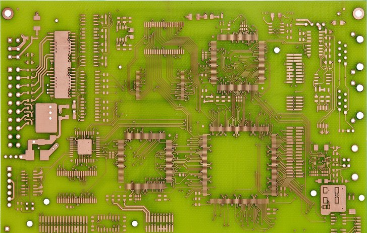
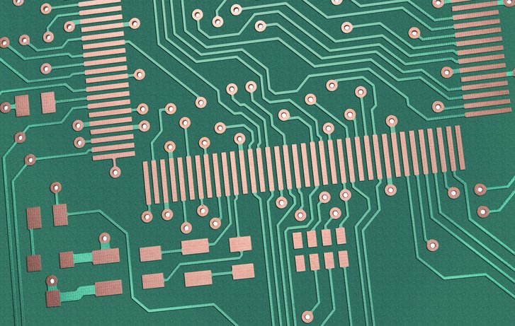
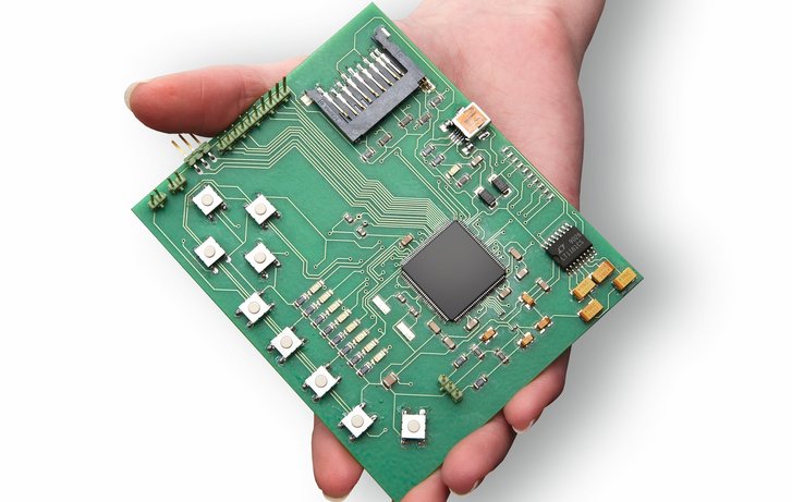
The complete line for PCB Prototyping

Research & In-house PCB Prototyping

The complete line
for PCB Prototyping

PCB prototyping process steps

Coordinated methods and tools from a single source

From structuring of the base material to complex production-level multilayers the entire prototyping process -- design, production, testing and optimization -- can be completed in a single day.

From layout data to fully functional PCB

LPKF offers easy-to-use, compatible solutions for all process steps.

Software with intuitive operation

Simple data preparation and machine control.

PCB structuring

Conductive tracks made by mechanical or laser-based systems within minutes.


PCB drilling

Drilling of through-holes and blind vias.

Through-hole plating

Through-hole plating without chemicals or with electroplating solutions.


PCB depaneling

Singulation of PCBs from larger panels for a wide range of PCB materials.


SMT / Finishing

Component population and professional finishing of PCB prototypes and small series.

Multilayers

Production of high-grade multilayer PCBs with up to eight layers in-house.

 Downloads

Catalog
Rapid PCB Prototyping Product Catalog (pdf - 3 MB)
Download
TechGuide
LPKF TechGuide PCB Prototyping (pdf - 3 MB)
Download

Training courses make the start simple

LPKF systems can be operated easily and intuitively

Detailed and understandable manuals lead and support the user during the installation, start-up and operation of the machines and software programs.

LPKF ProtoLasers are always installed by LPKF's own engineers. The user is familiarized with the possibilities of the system in a short training course.

We also offer installation and training for the smaller systems.  This training can be done at LPKF's premises or at your facility.

 Contact us

Your Contact Data

Your Message

I agree to the processing of my data pursuant to the Privacy Statement.

* Required fields
Productfinder
Productfinder