

")
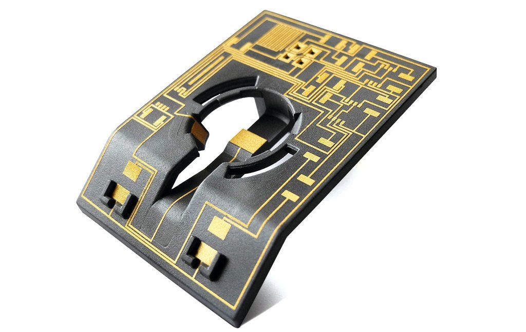
Injection-molded parts with structured conductive patterns
Completely 3D-capable: The laser beam defines the layout
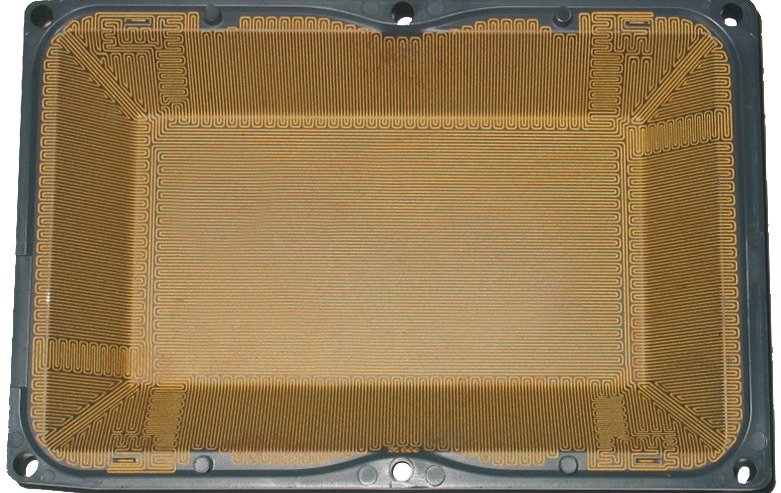
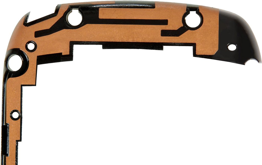
In the LDS process, the conductive trace is defined by a laser beam, which writes the layout right onto the injection-molded plastic element.
The injection-molded plastic contains a special LDS additive. This material is first injection-molded to form the required part. Then the laser beam exposes the areas in which the conductor structures will later be situated, thereby activating the additive. During the subsequent metallization in a copper bath, the conductive traces form in the activated areas with strong adhesion to the surface and sharp contours.In this way, different layers, for example, nickel and gold, silver, or soldering tin, can be built up successively.
Advantages for new products
- High degree of design freedom
- Miniaturization and weight reduction
- Integration of various functionalities (3D conductive trace structures, antennas, switches, connectors, and sensors)
- Shorter assembly times
- Fewer process steps
- Comparatively low initial costs
The patented LDS process
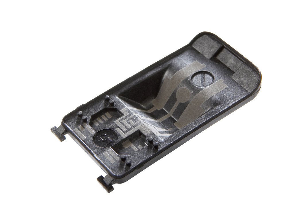
LDS process steps
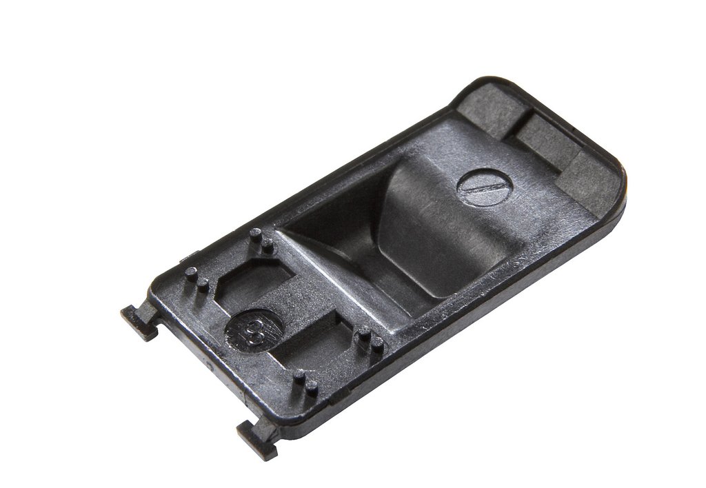
In this step, the laser beam structures the conductive pattern. The thermoplastic material is activated by the laser energy. A physical-chemical reaction produces metallic nuclei - this is the activation process. In addition to activation, the laser forms a microrough surface on which the copper firmly anchors itself during metallization.
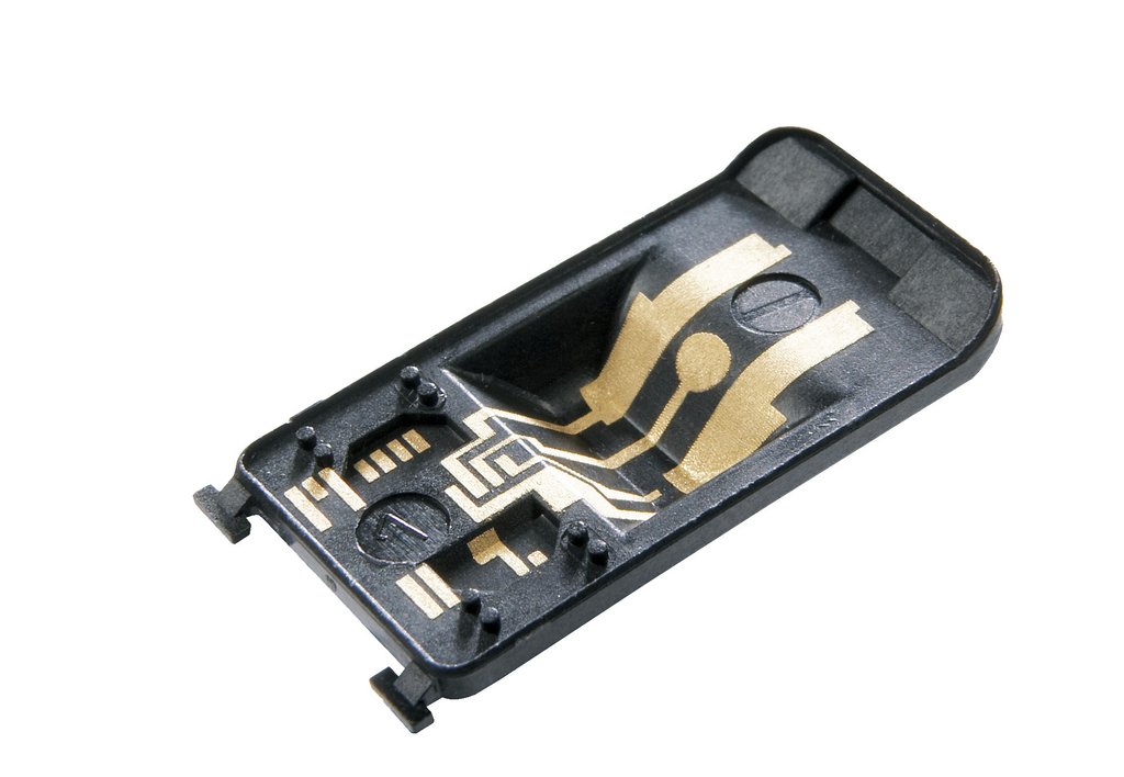
The metallization of LPKF LDS parts begins with a cleaning step. This is followed by an additive conductor build-up in electroless copper baths, typically in the order of 8 to 12 μm/h. Finally, an electroless application of nickel and a thin gold layer is usually carried out. Application-specific coatings such as Sn, Ag, Pd/Au, OSP etc. can also be applied in this process.
Many laser-activatable plastics with high heat resistance such as LCP, PA 6/6T or PBT/PET blend are reflow solderable and therefore compatible with standard SMT processes. For solder paste application, dispensing is the standard process when different height levels need to be reached. There are a number of suppliers of technical solutions for three-dimensional assembly.
LDS technology in use
Proven millions of times over
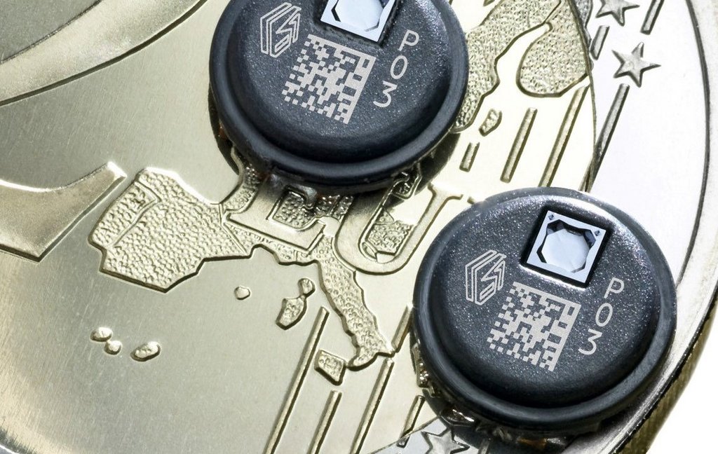
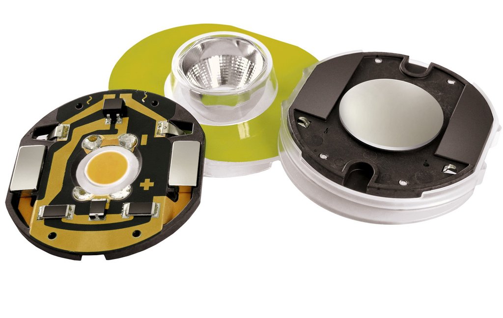
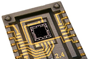
The LDS technology has been proven in numerous everyday applications. For example, it can be found in compact sensors such as pressure sensors. Cell phones also contain MIDs based on LDS technology. Millions of phones use these three-dimensional molded interconnect devices as space-saving integrated antennas. Other applications can be found, for instance, in medical, air-conditioning, and safety technology.
Through-hole plating
Reliable plated-through holes can be produced with LPKF LDS technology for connection of the surfaces of MIDs. This expands the possibilities for the layout.
Metallization
Various layers can be built up according to requirements.
- Chemical copper, nickel, and gold
- Electrolytic copper
- Flash gold
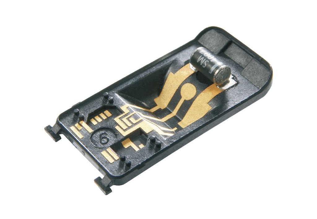
Assembly
Population with electronic components is possible after metallization.
- 3D assembly (pick & place)
- Vapor phase soldering
- Conductive adhesive bonding
- Aluminum wire bonding
- Flip chip process


WeLDS: New Options for the Electronics Industry

WeLDS: The unique combination of 3D-MIDs and laser plastic welding
WeLDS combines 3D-MIDs with laser plastic welding. LDS can be used to create conductive paths on the surface of injection molded parts. LPKF's laser plastic welding then ensures visually and functionally outstanding weld seams for durable and reliable connections of LDS components. The process thus offers revolutionary opportunities for further miniaturization and functional integration in the electronics industry.
- Efficient sealing and protection of 3D LDS components
- Higher geometric complexity of LDS parts
- Economical production
- High functional integration
The innovative WeLDS technology - already proven millions of times in series production.


