
 Grades for Active Mold Packaging (AMP)")
What is AMP?
AMP stands for Active Mold Packaging
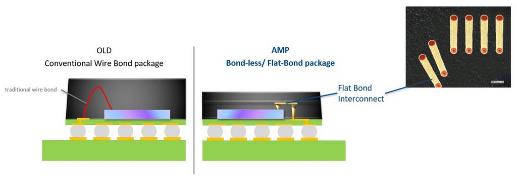
AMP establishes horizontal and vertical interconnect access between active and passive components in a heterogenous 2.5D packaging approach.
AMP is based on 3 proven and standardized, electronics manufacturing technologies.
1. Molding
Transfer- & Compression-Molding of thermo-set epoxy mold compound, doped with a laser-activateable additive.

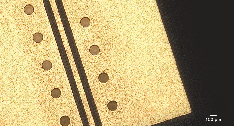
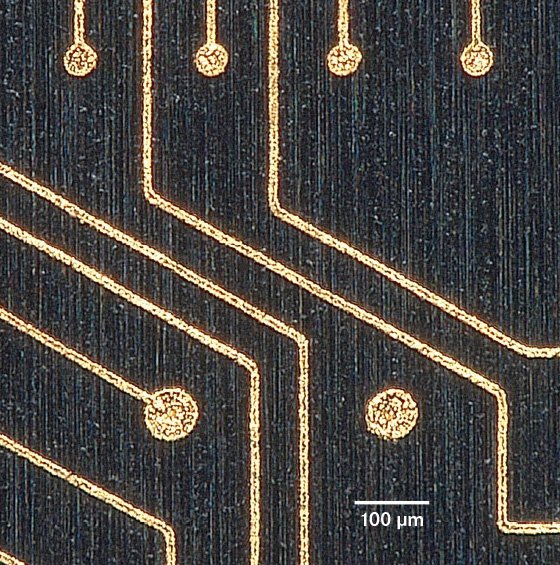
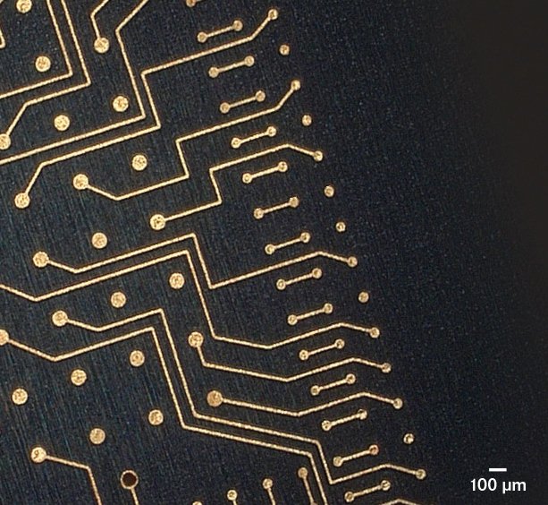
2. Laser Direct Structuring
Laser Direct Structuring and Drilling of the mold compound, activates the additive in the mold compound.

3. Electro-less plating
Electro-less plating deposits a conformal copper layer on only the laser activated areas of the compound.

Outstanding characteristics of AMP Technology
")

Active Mold Packaging (AMP) helps increasing the functional density of packages. AMP is very well suited for a selection of other mid-range applications requiring horizontal and vertical interconnects such as
Fine line/space conductive trace formation for Flip Chip Redistribution Layer (RDL) applications down to 25 µm
Medium sized conductive area formation for RF based Antenna-on/in Packages with operating frequencies up to 98 GHz
Large conductive area formation for conformal and compartment EMI shielding applications
Large bulk copper volume formation for heat dissipation and heat sink power package applications
Solderable conductive area formation for incorporation of passive components such as IPDs and SMD in SiP applications
| Epoxy Mold Compounds (EMC) | EMCs are based on thermoset polymers. Due to its excellent meachnical, chemical and electrical properties it is the most suited material for encapsulation. It's properties can be adjusted over a wide range satisfying the requirements of different applications, including RF-, logic-, discrete-, power-packages as well as for sensors and MEMS. |
| Laser-Direct Structuring (LDS) | The LDS technology has proven its versatility in RF-, medical-, sensing- and MEMS-applications. By offering the LDS technology in combination with compression-, transfer- and liquid molding of thermoset compounds it enables the use of the real-estate of the mold compound. The digital character of laser processing, allows for late design freezes and easy, fast and inexpensive circuitry layout changes. |
| Plating | The LDS technology does not require the formation of a seed layer via expensive PVD or CVD processes, just electro-less plating. For applications that require copper layers larger than 10um, a subsequent chemical plating step can be used too. |
...the transfer of the 2.5D circuit design from your Design Tool to the laser is digital. A quick change of the circuit design in your electronic design automation (EDA) tool, will change the pattern on the mold compound.
The digital character enables greater flexibility allows for very late design-freezes. Just in case the package's performance needed to be adjusted due to changed market demands.


Mold Compound Details

A selection of different Laser Direct Structuring - Epoxy Mold Compound (LDS-EMC) grades are available from major IC packaging compound suppliers. Through a close cooperation between LPKF and these suppliers, the compound formulation can be adjusted to your application specific compound requirements.