

Background and significance of the panel
Panels are used in electronics production to enable the partly simultaneous and more effective processing of several printed circuit boards. Each panel thus compromises several individual PCBs, which are arranged at a specific distance from each other and in an optimal arrangement to each other depending on the separation process.
In the panel composite, the circuit boards pass through all processing steps together, starting from the solder paste printing, over the assembly and until the final separation.
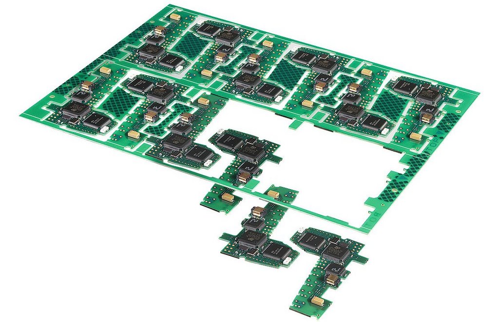
The adjacent figure shows an exapmple panel consisting of several assembled PCBs. Due to pre-milled channels, in this case the printed circuit boards have to be arranged with a larger distance from each other.
Types of panel
In general there are two different types of panels that can be used for the production of printed circuit boards. These differ with regard to the composition of the PCBs on the panel:
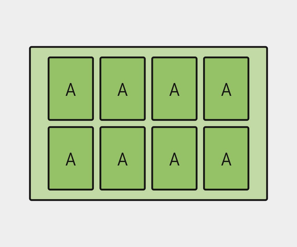
Homogenous composition (AAAA):
In homogenous assembly, the panel is composed of a multiplication of the same circuit board. This means that only one type of PCB is produced per panel. This is the most frequently used method in practice.
The popularity of this method is due to several important advantages: on the one hand, this method of assembly is independent of the manufacturing conditions and the product portfolio of the SMT manufactures. Secondly, the flexibility and effectiveness of the method is much higher than with any heterogenous composition of a panel.

Heterogenous composition (ABCD):
The panel is composed of a configurable mix of different printed circuit boards. This means that several types of PCBs can be produced simultanteously in a defined ratio.
An advantge of this composition is that stocks and buffers can be reduced with this method, since it is not necessary to provide a single panel for each type of PCB and a large number of PCBs do not have to be completed with each processing operation. On the other hand, it is difficult to control production differentiation and demand in a responsable way. For example, if a PCB is no longer needed, either the panel design would have to be changed or a large number of PCBs would be produced without demand.
Processes for depaneling
For cutting and singulating printed circuit boards, there is a selection of different separation processes. These are distinguished by different levels of costs, reliability and quality. The procedures include, among others:


Challenges of depaneling
Challenges
A central challenge in cutting is the respective geometry of the printed circuit board. Here the individual processes have different weaknesses. For example, saws are only able to make straight cuts. Milling machines are severely restricted with regard to minimum radii and thus their freedom of geometry. The laser, on the other hand, has limited use for material thicknesses of more than 2 mm. It must therefore be decided depending on the application context which method is most suitable.

In the various fields of application for printed circuit boards, such as medical technology, the requirements for technical cleanliness are constantly increasing and can often only be guaranteed by expensive subsequent cleaning processes. Especially during milling and other mechanical separation processes, dust is deposited on the PCBs, which can often lead to malfunctions and decrease the yield.
Another challenge in cutting PCBs is the individual equipment of printed circuit boards. Depending on the intended use of the PCB, various electronic components are placed on the top and/or bottm of the PCB. Defined by the cutting process, certain minimum distances between the components and the cutting line must be taken into account.
Structure of the panels
The type of composition and the selected depanelization process have a considerable influence on the panel structure. While the homogenous or heterogenous composition of the panel has a specific effect on the nesting, i.e. the general layout and arrangement of the PCBs in relation to each other, the depaneling process defines the distance between the individual PCBs.
Guidelines for panel design
The interval in which the size of the panel can vary is usually defined by some machines in the production chain of printed circuit boards, such as solder past printers, pick-and-place or quality inspection machines (AOI). Therefore, panel sizes smaller than 2 inches or about 50 mm cannot be processed due to the conveyor width. To avoid this problem, either free areas at the edges must be added or additional PCBs must be arranged on the panel. In contrast, the maximum dimensions of the panels are also determined by the machines. For most models, the maximum dimensions correspond to standardized panel sizes such as 12" x 18" (approx. 305 mm x 460 mm).

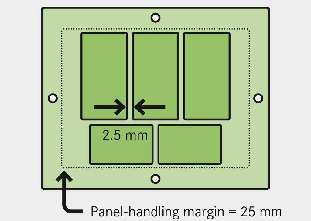
Especially flexible, but also many rigid PCBs have to meet the requirements of limited installation space and therefore have irregular and non-linear contours. In oder to be able to transport the panels with the conveyors and to simplify handling, however, they must have two parallel and straight edges. Therefore, an otherwise unused handling edge (marked light green in the picture) must be added around the irregular contours. The shape of the panel also allows conclusions to be drawn about the cutting process to be used, since saws and milling machines, for example, have strict limitations with regard to their geometric freedom.
To ensure practical handling of the panels for the individual production steps, a narrow strip must be left free all around the edge of the panel. In this way, the panels can be transported more easily with conveyors, transport belts and similar aids.
The width of the edge varies depending on the structure of the panel: for simple structures (one-sided/two-sided) about 12.5 mm (0.5 inch) and for multilayer boards about 25 mm (1 inch). In the case of multilayer boards, more space is required because holes have to be provided for the alignment of the lamination (figure below). The respective width should be checked depending on the machines used in the PCB production and taken into account in the design phase of the panel.

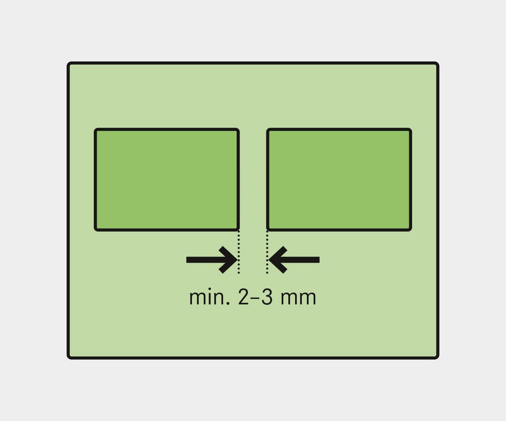
Depending on the separation method used, the distances to be maintained between the individual circuit boards can vary greatly. In case of milling, for example, the channels alone have a width of about 2-3 mm. In contrast, the distances can be reduced to a minimum of a few hundred µm for laser depaneling. As a rule, and especially with small dimensions, these savings mean that considerably more PCBs can be placed per panel.
When separating the circuit boards, not only the distances between the PCBs but also the distances from the cutting edge to the mounted components must be considered. Especially the height of the components is decisive in this case. As a tendency, larger distances must also be maintained for higher components on the circuit board. Even in this case the distances to be considered vary depending on the cutting method and tool. Since the laser beam is considerably narrower than a milling head or saw blade, space on the panel can also be saved here. As a rule, even sensitive components can be positioned at a distance of about 100 µm from the cutting edge without being subjected to mechanical or thermal stress.

Another guideline for the economic panel design is the appropriate preparation of the panel for the final separation. This increases the speed at which the individual boards are finally separated from the panel. Two approaches are widely used here, which are presented in the following:
Breakout-Tabs
Breakout-Tabs are one way to prepare the panel in advance for the final cutting process and to increase the cutting speed and throughput time. In this case, a pre-milled channel is located around the respective circuit boards, which has gaps at predefined points where material is left behind. These gaps can also be filled by so-called "mouse bites" at the lower and/or upper edge. These are small drill holes that are arranged at fixed distances between the respective milling channels.
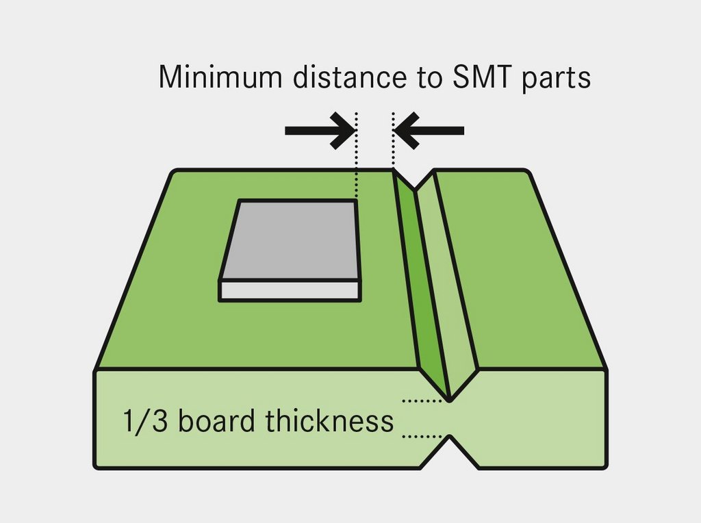
V-Groove:
An equally widespread method for preparing the separation process of the panels is the so-called V-Groove. With this method, the panel is cut from below and above at the same position, whereby about1/3 of the material is removed from each side. Especially in mechanical processes, the induction of mechanical stresses can be reduced in this way. Overal, the final cutting process is accelerated, since logically only one third of the material needs to be cut.
Disadvantages of the process are that it is only suitable to a limited extent for high mounting and overhanging components and that it only produces straight cutting edges.

Another possibility for separation is to cut the circuit boards without preparatory measures such as V-grooves or tabs. Laser depaneling in particular offers significant advantages for the so-called full cut of the PCBs, since the width of the cutting channel and cutting tool are of central importance here. For comparison: while the laser beam requires a cutting channel that is about 200 µm wide, the milling machine requires depending on the tool between 2000 and 3000 µm.
The savings achieved by this difference make it possible to place considerably more PCBs per panel, especially for smaller PCBs and larger panels. The producer thus saves in two ways: directly by saving on materials and indirectly by more effective processing of the panel during further processes in the PCB production.
Conclusion
It has been shown that the design of the panel is a complex project in which a number of influential factors must be taken into account. These have a significant impact on the cost, quality and profitability of the PCB production. In particular, the choice of the separation process is of central importance for the design and the maximum utilization of the panel. Here mechanical processes are associated with significant limitations.
With the help of this page we have tried to give you some guidelines to support you in your work. In the download area we have summarized these for you once again in one document.
If you have any questions or suggestions, please contact us using the contact form.