

Additive coatings of ceramics
There are various methods for creating conductive structures on ceramics. Electroless copper plating of selected areas has not been part of this until now, because the good chemical resistance prevented adequate adhesion. However, experiments with excimer lasers in the past have confirmed the basic possibilities for such a coating process.
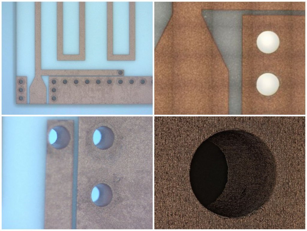
LPKF has extensive knowledge of material activation from LDS technology and, with the LPKF ProtoLaser S4, also has a laser system that demonstrates its capabilities in ceramic processing on a daily basis. So, what happens when a ceramic substrate is structured and drilled with a laser (nanoseconds, 532 nm wavelength)? Can a sufficiently adhesive and homogeneous copper layer then be built up in the structured areas?
The tests were extremely positive. The layout of the laser activation could easily be prepared in the LPKF CircuitPro system software supplied. Tests with different laser parameters quickly brought good structuring results for the processed carrier.
In the experiment, a double-sided antenna was produced on Al2O3 with a final dimension of 26 x 26 mm. The same laser system created registration holes outside the layout area for exact layout positioning on the front and back. The holes for the through-hole plating were also carried out by laser during processing.
The processing time for pass holes, double-sided structuring with a depth of 18 µm and through-plating holes was a total of just 25 minutes. A homogeneous copper layer was then built up in an electroless activation bath, which is connected at least in a scratch-resistant manner.
Such initial layers take on the necessary electronic functions directly or are galvanically amplified, assuming an appropriate layout. The LPKF ProtoLaser S4 used for structuring can then take over the separation of contacts that are no longer required.
The experiment proves that ceramics can be structured and activated safely and quickly in-house using standard LPKF ProtoLasers and tried-and-tested LDS technology can. In this way, new product layouts and prototyping processes for three-dimensional RF components can be realized with already known follow-up processes.
The full post can be found at the LPKF knowledge-center.